The Designer's Guide Community Forum
https://designers-guide.org/forum/YaBB.pl
Simulators >> RF Simulators >> IIP3 simulation
https://designers-guide.org/forum/YaBB.pl?num=1168247204

Message started by aaron_do on Jan 8th, 2007, 1:06am

Title: IIP3 simulation
Post by aaron_do on Jan 8th, 2007, 1:06am

Hi all,

i'm trying to simulate the IIP3 of my LNA and i found what appears to be a problem with the simulator. I'm using cadence spectrerf. I've tried 2 methods.

1) PSS and PAC
2) two tones in PSS

I observed the same problem in both instances.

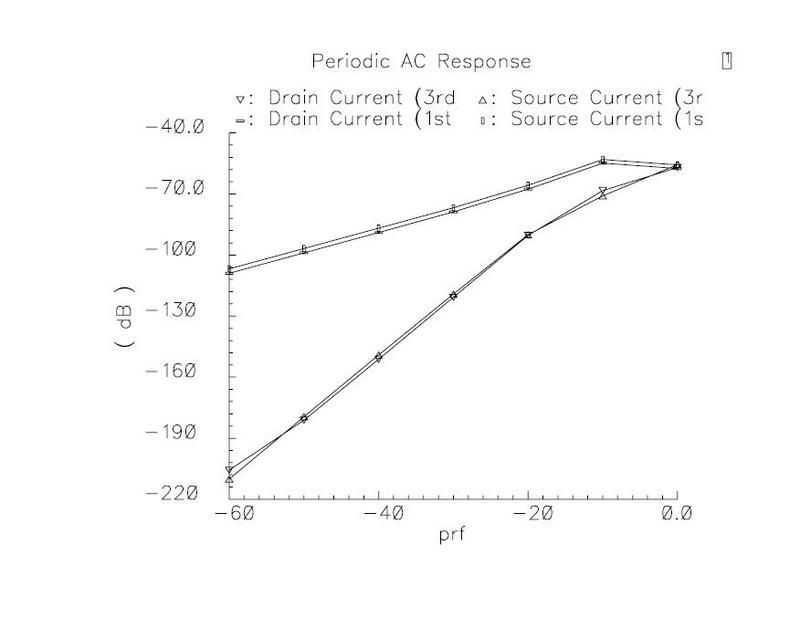
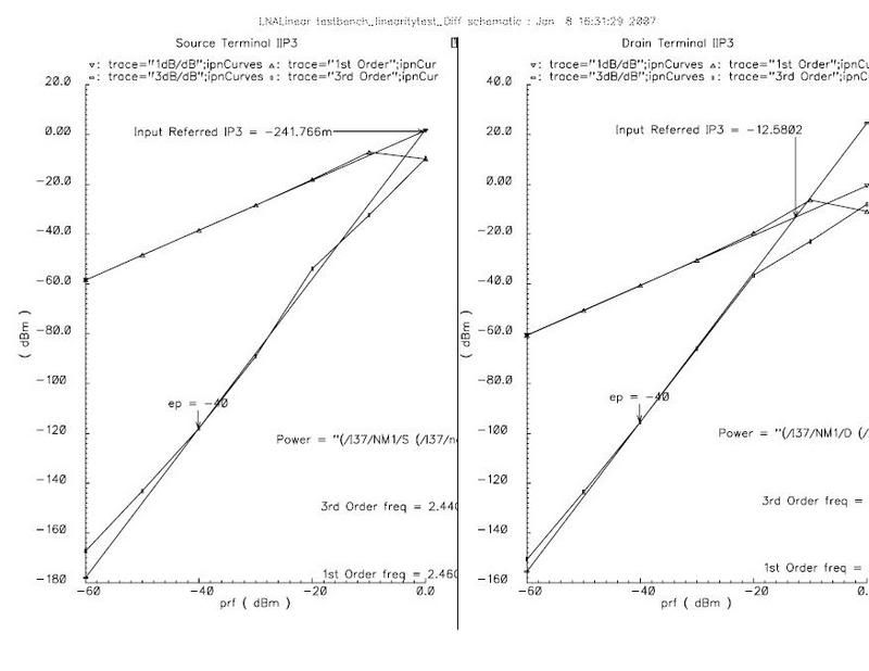
My LNA is a cascode LNA in CMOS. For the cascode transistor, I found the IIP3 to be significantly worse when measured from the drain terminal than the source terminal. However when I try to plot the current from the PSS or PAC simulation there doesn't seem to be a difference between the drain and source terminal.

The only possible explanation is that the load is extremely non-linear. The voltage waveform appears to follow the same shape as the current waveform however.

Here are two pictures of the simulation results. The first is the plots of the 1st and 3rd harmonics from the drain and source terminal. The second is the IIP3 from the same terminals. The third order harmonic is clearly significantly worse in the IIP3 simulation when measured from the drain terminal. Has anyone encountered a similar problem or is it likely that my load is really causing this problem. I've used a PMOS load with CMFB.


thanks,
Aaron

Title: Re: IIP3 simulation
Post by ACWWong on Jan 8th, 2007, 3:10am

My thoughts are:
The cascode source is low impedance... so voltage swing is low and so distortion effects are low. The current is source and drain are largely the same as expected.
The cascode drain is terminated by a load impedance, in your case PMOS with CMFB... you say the voltage waveforms (you can access the time_domain wavforms in pss to see the pss solution) don't look distorted at the drain ?? Is the first order slope even correct (ie gain)? Was your CMFB designed to handle the volatge swings you are subjecting it to ?
Anyway you can simply remove the PMOS/CMFB loading and replace with resistors (you can artifically increase supply to ensure you get the correct DC drop, and enough headroom for voltage swings up and down upto the signal levels of interest) and check again.
cheers
aw

Title: Re: IIP3 simulation
Post by aaron_do on Jan 8th, 2007, 6:09pm

thanks aw,

I'll keep looking into it but i guess it really is a problem with the PMOS loads.

thanks,
Aaron

The Designer's Guide Community Forum » Powered by YaBB 2.2.2!
YaBB © 2000-2008. All Rights Reserved.