Post by iVenky on Apr 15th, 2013, 9:25pm
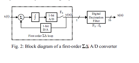
Well the above one is the basic block diagram of a first order sigma delta ADC. Now I am trying to implement that in hardware. Here's the image that I saw regarding the implementation in hardware. I have few doubts here. The integrator that is present in the block diagram above is not present in the circuit below but rather we have a RC integrator at the output of DAC which is not the case above. I tried this circuit and I am getting the Delta modulated signal at the output of the DFF. But my question is this- Will we get the same noise shaping as that of the basic block diagram? I am having a doubt because both circuits seem to be different. Will we get the same maximum possible SNR for both circuits for a given OSR?

Thanks a lot