Post by baab on Feb 20th, 2014, 11:32pm
Hi,
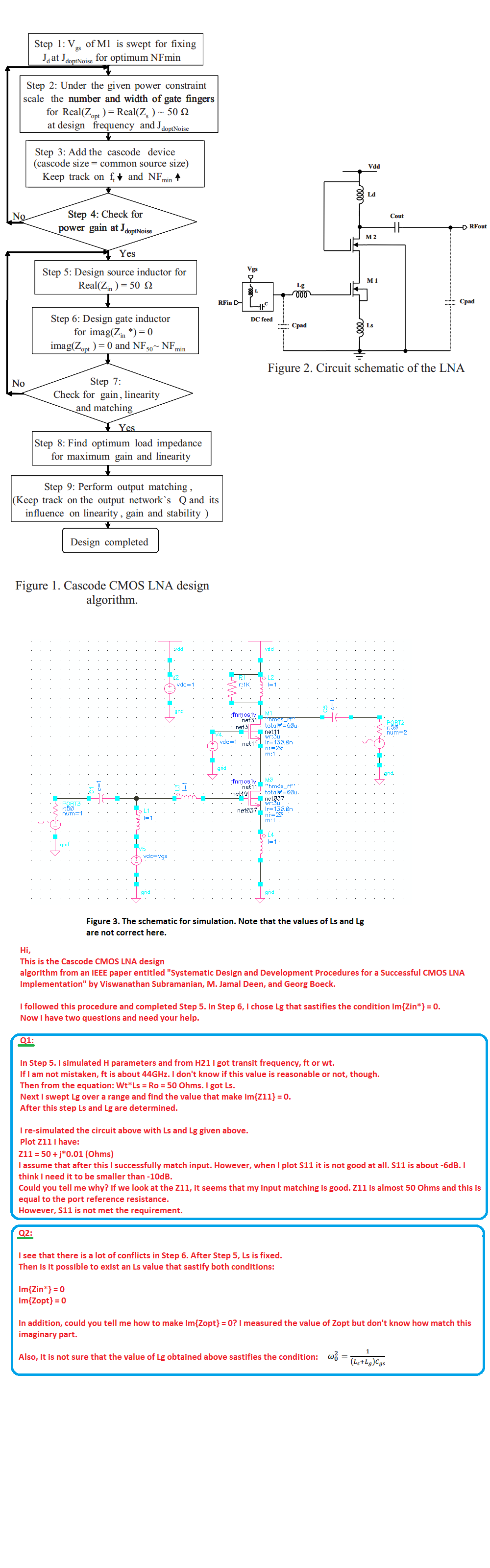
I am getting some problems relating to input impedance matching.
Please help me with questions in the picture. Thank you.
|
The Designer's Guide Community Forum
https://designers-guide.org/forum/YaBB.pl Design >> RF Design >> S11 and Z11 problem for input impedance matching https://designers-guide.org/forum/YaBB.pl?num=1392967942 Message started by baab on Feb 20th, 2014, 11:32pm |
|
Title: S11 and Z11 problem for input impedance matching Post by baab on Feb 20th, 2014, 11:32pm Hi, I am getting some problems relating to input impedance matching. Please help me with questions in the picture. Thank you.
|
|
Title: Re: S11 and Z11 problem for input impedance matching Post by aaron_do on Feb 23rd, 2014, 9:04pm Hi baab, 1) as I mentioned before, Z-parameters are determined with high-impedance ports while s-parameters are determined with matched ports. So based on the following equation, you can see why your amplifier S11 doesn't match when Z11 is 50ohm.  *equation can be found at http://en.wikipedia.org/wiki/Scattering_parameters Probably in your case, S22 is very bad, so even though S12 is good, the amount of reflection is enough to significantly degrade S11. You can work around this by doing only a 1-port simulation to match Z11, but keep the load connected. 2) As far as I remember, the inductive source degeneration amplifier cannot get you simultaneous matching of Zopt for NF and power. i.e. you can't get Im{Zopt} = 0. But it is possible to get it quite close. I think you need to adjust the value of Cgs with an extra capacitor. 3) The step-by-step LNA design procedure doesn't look quite right to me. A lot of it is right, but there are parts that are weird. For example, Step 7, check for gain, linearity, and matching. If it doesn't meet requirements go back to step 5. But step 5 doesn't have any room for adjustment since there is only one possible value of Ls. So what is the point in going back to step 5? regards, Aaron |
|
Title: Re: S11 and Z11 problem for input impedance matching Post by baab on Feb 25th, 2014, 1:47am Thank you, Aaron! I need to read it more before replying. |
|
Title: Re: S11 and Z11 problem for input impedance matching Post by baab on Mar 8th, 2014, 11:09pm Hello, Aaron. I spent a lot of time reading about it. As from what you said, I realised that my mistake is that I used Z11 instead of Zin for input impedance matching. I intended to do the input matching first and then output matching. However, because Zin depends on output, I now think I need to match output first. Now it seems to be a vicious circle here. To match output, I need to know Zout but once again Zout also depends on input. I don't know how can I match input/ouput now. They interact each other. |
|
Title: Re: S11 and Z11 problem for input impedance matching Post by baab on Mar 8th, 2014, 11:18pm According to the analysis, Zin doesn't depend on output network at all. I will simulate to check it now. |
|
Title: Re: S11 and Z11 problem for input impedance matching Post by baab on Mar 9th, 2014, 5:24pm Hi, I have two problems needing your help. 1. Is there a way to measure input impedance without having to do output impedance matching first? 2. S11 is input reflection coefficient when output is matched. I am wondering how Candence do that? The output port impedance is 50 ohms and Zout is not 50 ohms. (considering the circuit posted above without input and output match networks) I thought that we can only measure S11 and S22 as input and output have already matched. However, it doesn't seem to be the case. |
|
Title: Re: S11 and Z11 problem for input impedance matching Post by aaron_do on Mar 9th, 2014, 6:00pm Hi baab, 1. Do it iteratively. For example, start off with a reasonable estimate for the output matching network, and then do input matching, and then adjust your output matching network again, and finally readjust your input matching network. It will only take one or two iterations depending on how good your initial estimates are. Quote:
2. This statement is incorrect. S11 is the input reflection coefficient when there is no reflection at the load. i.e. ΓL = 0. Cadence doesn't need to know the details of your circuit. Note that Z11 is measured with ZL = ∞. i.e. ΓL = 1. regards, Aaron |
|
Title: Re: S11 and Z11 problem for input impedance matching Post by baab on Mar 9th, 2014, 7:20pm Hi, Aaron. Quote:
no reflection at the load = output is matched??? Can I convert S parameters to Z parameters and use Z11 as input impedance with the condition that output is matched? |
|
Title: Re: S11 and Z11 problem for input impedance matching Post by aaron_do on Mar 9th, 2014, 7:52pm Hi baab, Quote:
Nope. You seem to be confusing the output and the load. Don't worry, everybody has this confusion when they are starting out. The output impedance is looking from the 50-ohm load back into the circuit. It is basically a parallel combination of your transistor output impedance and the inductor's impedance. The load impedance is the next circuit block. For example, in your case it is probably a mixer. In textbooks, the load impedance is set to 50-ohm, but in practice there is no such requirement. It might help if you imagine that there is a transmission line connected between the source and the DUT, and the DUT and the load. Like so, RS ------tline (Z01)------DUT------tline (Z02)------RL Here is the sequence of events from the output side: t1: DUT generates output wave on tline (Z02) t2: output wave reaches load. For ZL = Z02, RL = 0 and therefore there is no reflection (end - this is the case for S11 analysis), otherwise go to t3. t3: there is some reflection at the load (ΓL), and this travels backwards down the tline (Z02) to the DUT output. t4: upon reaching the DUT output, there is some transmission back to the input (S12), and if Zout ≠ Z02, there is some re-reflection. t5: so this basically goes on for ever with the signal getting smaller and smaller as it is absorbed by all the loss and load. In reality, the reflection coefficient should be defined wrt the transmission line since reflection is only a meaningful concept when the distance traveled by the signal is long enough for it to experience a time delay. So in this case, the load reflection coefficient would be defined by the mismatch between Z02 and RL. However, for spectre's SP analysis, Z02 is actually defined by RL. Therefore ΓL in the simulation is by definition equal to zero. So if you were to use a 1-kohm impedance for the load port, then for S11, the load would be 1 kohm, but for Z11, it would be infinite. A good reference if you want to understand this properly is "Power Waves and the Scattering Matrix" (I'm just quoting that from memory, so you'll have to look around"). Its quite an old paper. regards, Aaron |
|
Title: Re: S11 and Z11 problem for input impedance matching Post by baab on Mar 10th, 2014, 10:57am Thanks a lot, Aaron. I misunderstood between output and load. There is one thing that I don't get from your answer. Quote:
Shouldn't it be RL = Z02? I suppose that the characteristic impedance Z02 is real. |
|
Title: Re: S11 and Z11 problem for input impedance matching Post by baab on Mar 10th, 2014, 11:27am I inserted a output matching network between the output of transistor and the output port. Let's call input reflection coefficients, S11 and S'11 correspond with two cases, before and after adding output matching network, respectively. From measurement, I see that S'11 is different from S11. And as I know, we can convert S11 and S'11 to Zin. S11 is NOT equal S'11 and this means that Zin also changes as output matching network is added. I am wondering why that is the case. Why Zin is affected by output matching network? There is little feedback here. (I suppose this is correct because the cascode topology is used.) From the circuit, Zin only depends on Ls, Lg, Cgs, and gm. Could you explain? |
|
Title: Re: S11 and Z11 problem for input impedance matching Post by aaron_do on Mar 10th, 2014, 6:01pm Hi baab, Quote:
sorry for the typo. I meant For ZL = Z02, ΓL = 0 Quote:
How did you calculate Zin? Is it Z11? is the difference in Zin large or small? As I have explained previously, when using Z11, ΓL = ∞, so it could explain a small, and maybe even moderate difference in Z11. When you say there is little feedback, what is S12? The calculation of Zin in your diagram makes a lot of simplifying assumptions. That's why it doesn't depend on the load...... Aaron |
|
Title: Re: S11 and Z11 problem for input impedance matching Post by baab on Mar 10th, 2014, 8:28pm Hi, Aaron. Quote:
I plotted S11 in smith chart and then move the pointer over the point and read that corresponding impedance value. I think that is Zin of the circuit with the condition there is no reflection from load. I also used ZM analysis to find Zin and the two methods give the same result. Quote:
No, Z11 is the input impedance as load is open, RL = ∞ while Zin here is measured as there is no reflection from load. Quote:
It is very large. Quote:
I haven't measured it yet. I was only interested in S11 and S22. I thought that the cascode topology will always give good isolation or very small S12 no matter how good the input/output matching is. Quote:
I don't understand why Zin changes largely as output impedance matching is added. I supposed it should be very small change. |
|
Title: Re: S11 and Z11 problem for input impedance matching Post by aaron_do on Mar 10th, 2014, 10:10pm Hi baab, if you set up the simulation and circuit properly, then it should be a small change. You're just going to have to look over your circuit carefully to find the problem. For example, make sure the biasing point doesn't change. The more information you post, the more people can help. regards, Aaron |
|
Title: Re: S11 and Z11 problem for input impedance matching Post by baab on Mar 11th, 2014, 1:33am Thank you, Aaron. Here is my circuit for simulation and simulation results. 1. Before adding output matching network Zin = ZM1 = 109.1 - j 33.01 S11 = -7.604dB S22 = -1.739dB 2. After adding output matching network Zin = ZM1 = 50 - j5.711*10^-4 S11 = -99.19dB S22 = -12.43dB As you can see, S22 is not so good. Therefore, I did output matching again but after getting good S22, S11 is very bad. It is about -2dB. |
|
Title: Re: S11 and Z11 problem for input impedance matching Post by aaron_do on Mar 11th, 2014, 9:46pm Hi baab, before looking any further, why don't you first verify that S12 is indeed very good. For example, S12*S21 should be better than -10 dB. regards, Aaron |
|
Title: Re: S11 and Z11 problem for input impedance matching Post by baab on Mar 12th, 2014, 12:00am Hi, Aaron. Here are S-parameters for the circuit after adding output matching network: S11 = -99.19 dB S12 = -35.86 dB S21 = 23 dB S22 = -12.43dB I think S12 is good here. There is only one problem is S22. It is not really good. |
|
Title: Re: S11 and Z11 problem for input impedance matching Post by baab on Mar 12th, 2014, 2:16am Hi, Aaron. I followed your advice, do the input/output matching iteratively. Now I got S11, S22, S12 and S21 fairly good. I need to replace all ideal components with practical ones in TSMC and use band pass filter for output matching. Thank you. |
|
Title: Re: S11 and Z11 problem for input impedance matching Post by aaron_do on Mar 12th, 2014, 2:17am Hi baab, so after improving S22 further, S11 degrades down to -2 dB? That sounds quite odd. Seems like I've missed something. I'll think about it, but let me know if you figure it out... BTW, I assume you are checking the same frequency every time. Also, -12 dB isn't bad... Aaron |
|
Title: Re: S11 and Z11 problem for input impedance matching Post by aaron_do on Mar 12th, 2014, 2:46am Good to hear! But after looking again at one of your previous posts, you mentioned that after adding an output matching network, S11 improved from -7.6 dB to -99 dB. Is that just a typo and you meant after adding an input matching network? Or did you accidentally switch the ports... :P Anyway since you got it working, don't worry about it... Aaron |
|
Title: Re: S11 and Z11 problem for input impedance matching Post by baab on Mar 12th, 2014, 3:08am aaron_do wrote on Mar 12th, 2014, 2:46am:
Hi, Aaron. I intended to mention it before but didn't. I did input/output matching as follows. 1. Do output matching first. After this I got really good S22. I don't remember now but it is very small. 2. Do the input matching by choosing the appropriate values of Ls and Lg. After this I got a very good S11, it is about -99dB. However, S22 now degraded. Now, input matching is really good while output one is not so good. When I wrote that post, I used this circuit along with all values calculated above. I remeasured S parameters like this: Before adding output matching network: I removed the output matching and measure S parameters. After adding output matching network: I recovered the output matching calculated previously and measured S parameters. That explained why S11 is good after adding output network. I think the replacement of TSMC components will cause many changes and I need to optimize again. By the way, I just measure the power consumption. It is about 8mW. Do you think it is too large? I am thinking about reducing it by lowering bias voltage Vgs. I choosed Vgs = 0.6V. |
|
Title: Re: S11 and Z11 problem for input impedance matching Post by aaron_do on Mar 12th, 2014, 5:01am Hi baab, you need to adjust the power consumption based on your noise and linearity requirements. If you are well above specs then consider reducing the power consumption. Whether 8mA is high or not depends on your application. regards, Aaron |
|
Title: Re: S11 and Z11 problem for input impedance matching Post by baab on Mar 12th, 2014, 7:31pm Hi, Aaron. I replaced ideal components by the real ones. With Ls and Lg TSMC components, there is no significant change in S11 and S22. However, I am struggling with the inductor in series with bias voltage Vgs. It is 1H. But as you said, it is impossible to do it in TSMC. I tried to do replace it by an inductor in TSMC with the same inductance. The result is that S11 and S22 changed completely. It is almost unacceptable. S11 is about 0dB while S22 is -6dB. I hope you could help me out. I just replaced it by a resistor 10K and the S11 and S22 are good at the orignal. However, resistor 10K is also impossible. |
|
Title: Re: S11 and Z11 problem for input impedance matching Post by aaron_do on Mar 12th, 2014, 8:29pm Hi baab, a 10kohm resistor is easy to implement. You can use the real on in your PDK. regards, Aaron |
|
Title: Re: S11 and Z11 problem for input impedance matching Post by baab on Mar 13th, 2014, 2:00am Hi Aaron. I am glad that we can use the 10K resistor. However, I am having a problem with the inductor at the output (the one in parallel with 1K resistor). I tried to replace it by an inductor TSMC with the same inductance 1H. However, the results are terrible. NF increased significantly from 1dB to 15dB. S11, S12 degraded to about -2 or -3 dB. I am wondering why 1H inductor TSMC 0.13um and 1H ideal inductor from AnalogLib can cause a great difference like that. |
|
Title: Re: S11 and Z11 problem for input impedance matching Post by aaron_do on Mar 13th, 2014, 4:53am Hi baab, 1H is impossible to implement. You need to re-design your matching network. The easiest way to do it is to use one shunt inductor and one series capacitor. The shunt inductor will replace the 1 H inductor. regards, Aaron |
|
Title: Re: S11 and Z11 problem for input impedance matching Post by baab on Mar 13th, 2014, 7:29pm Hi, Aaron. I think that will change almost completely my components values. Now. I'd like to ask some questions before making any changes. 1. In the circuit posted above, there is a resistor 1K in parallel with an ideal inductor 1H at the drain of cascode transistor. As you said before, the resistor is a parasitic component of the inductor not actually a separated resistor itself. I am wondering why don't we put a high resistor at drain to get a very high voltage gain. Av = gm* Rd => If we put a high Rd, for example, 10K, then the voltage gain or S21 will be very large. As I know, if we use Rd from parasitic component, it won't be as large as the separated one. 2. Is 1F capacitance implementable in TSMC 0,13um? If not, then I also need to replace all input/output coupling capacitors with the real ones. And, for example, because 1F capacitor doesn't exist. I will have to use capacitors of much smaller capacitance. Therefore, these coupling capacitors will affect significantly to the input/output matching networks. I will have to take them into account. They are part of input/output matching networks. 3. In my case fc is about 1.5GHz and bandwidth = 20MHz. I am considering about bandpass matching network at the output. I attached my schematic below. Could you confirm if this is right? Thanks. |
|
Title: Re: S11 and Z11 problem for input impedance matching Post by aaron_do on Mar 13th, 2014, 8:47pm Hi baab, yes you will need to completely change your component values. 1. You can use a resistor, but the value of the resistor will be constrained by the DC drop across it. You will save some space using a resistor, but the performance will probably be better using an inductor. 2. 1 F is also no implementable. Anything more than a few pF is starting to get large. The reason I recommend that you use a shunt inductor followed by a series cap is that these components can be used to replace your ideal ones. 3. For an LNA there is usually no need to constrain the bandwidth. Just make it as wide as is convenient. In fact, if your system bandwidth is 20 MHz, your LNA bandwidth should be much wider to account for modeling errors or PVT. The network I suggested above is a high-pass network. It is the easiest network to implement. Usually the reason you would use more than one inductor/capacitor in your network would be to widen the bandwidth of the matching network, but for a narrowband system it probably isn't necessary. regards, Aaron |
|
Title: Re: S11 and Z11 problem for input impedance matching Post by baab on Mar 14th, 2014, 7:04pm Hi, Aaron. Now, I don't know where to start. The ideal case seems much simpler. I think first, we need to choose the width of transistors to get noise matching. However, with this practical case, the inductors and capacitors also include internal resistance and they affects significantly to optimum noise impedance. The problem is that I can't know in advance these internal resistance and can't simulate to get NFmin. |
|
Title: Re: S11 and Z11 problem for input impedance matching Post by baab on Mar 17th, 2014, 2:24am Hi, Quote:
How about using a 1K resistor in parallel with an inductor from TSMC 0.13um? And then there is also no DC drop and in the same time we can increase voltage gain as the equivalent total resistance at the drain increases. |
|
Title: Re: S11 and Z11 problem for input impedance matching Post by baab on Mar 17th, 2014, 7:06am Hi Aaron. I replaced almost all components by TSMC 0.13um except for the inductor in parallel with 1K resistor. However, this is my new problem. 1. Can I use an inductor from TSMC 0.13 and connected it in parallel with a external resistor 1K? 2. If #1 is possible, then I need to use the inductor with inductance > 1uH. As you said, it seems to big. How can I solve this/ |
|
Title: Re: S11 and Z11 problem for input impedance matching Post by aaron_do on Mar 17th, 2014, 6:01pm Hi baab, the only way you can get that 1 uH inductor is to have it off-chip. But you don't need to do that. Instead you should change your matching network. You seem to have chosen a very complicated matching network. How did you choose the values? Why don't you just use one shunt inductor to replace the 1u inductor, and then a series capacitor? If you do this, the value of the inductance will be much more reasonable. Also, the 1kohm resistor can be absorbed into the parasitic resistance of the inductor. regards, Aaron |
|
Title: Re: S11 and Z11 problem for input impedance matching Post by baab on Mar 18th, 2014, 2:52am Hi Aaron. I did exactly the circuit you suggested. However, because the parasitic resistance too small, the voltage gain S21 is so low. I don't have the picture right now. I will post it later. |
|
Title: Re: S11 and Z11 problem for input impedance matching Post by aaron_do on Mar 18th, 2014, 6:21am Hi baab, that doesn't sound right. If S21 was not good then you most likely chose your component values wrongly. regards, Aaron |
|
Title: Re: S11 and Z11 problem for input impedance matching Post by baab on Mar 20th, 2014, 1:53am Hi, Aaron. This is my circuit. I used the circuit as you suggested. However, my problem is about drain inductor. It should be larger than 1uH to get a good S12, S21, S11, S22. If I change Ld to the one with much smaller inductance then all S parameters will be degraded. I know that the impedance matching networks are not correct. However, that will completely change my circuit. Please help me with the following. 1. Is the output matching network above the one you suggested? 2. What are the criteria in choosing coupling capacitors? These coupling capacitors are parts of input and output matching networks. I think we need to choose these capacitors first. (my frequency is about 1.5GHz) |
|
Title: Re: S11 and Z11 problem for input impedance matching Post by aaron_do on Mar 20th, 2014, 6:09pm Hi baab, you made quite a big error there. In your circuit, L0 is shorting the drain of M1 to ground (i.e. the biasing point is wrong). For the circuit I'm trying to describe, you should remove L17 and use L0 in its place. That way you won't need the 1uH inductor. Also, as you say, C1 will become part of the matching network. regards, Aaron |
|
Title: Re: S11 and Z11 problem for input impedance matching Post by baab on Mar 20th, 2014, 10:29pm Hi, Aaron. You are right. The simulator caused an error and I put a 1ohms in series with that inductor only for simulation purpose. I thought that that is only a problem with simulation. In real world, that is not problem at all. I'd like to ask about coupling capacitors. What are criteria in choosing these ones? Assuming that my frequency is about 1.5GHz. I consulted some papers and calculated the impedance Zc = 1/wC of that capacitors at interested frequencies and the results are different. Zc ranges from 1ohm to 120 ohms. That is quite big. |
|
Title: Re: S11 and Z11 problem for input impedance matching Post by aaron_do on Mar 21st, 2014, 2:02am Hi baab, Quote:
What do you mean? In the real world it is still a problem. You can't put an inductor where L0 is... Quote:
It depends on your design. The capacitors should be large enough not to cause any significant performance loss. But you don't want them to take up too much area. regards, Aaron |
|
Title: Re: S11 and Z11 problem for input impedance matching Post by baab on Mar 21st, 2014, 2:22am Thank you, Aaron. Quote:
In real world, L0 is not purely inductive. Therefore, there is resistance and no DC short there. This is what I thought. Quote:
Yes, that is what I confused. Based in layout, I think I can estimate the upper limitation for these capacitors. However, how about lower limit? I am still not sure how to calculate it. The larger the capacitance the smaller its reactance and the better performance. How to know that a capacitance causes significant performance loss or not? For example, my frequency is 1.5GHz and C = 1pF. Is that good? |
|
Title: Re: S11 and Z11 problem for input impedance matching Post by aaron_do on Mar 21st, 2014, 6:39pm Hi baab, Whether L0 is purely inductive or not it is gonna mess up your DC operating point. Taking C0 as an example, it is in series with L2. L2 and C0 will resonate at some frequency, below which the combination will act like a capacitor rather than an inductor. So make sure the resonance is much lower than your operating frequency. Just make sure there are problems with your s-parameters. Aaron |
|
Title: Re: S11 and Z11 problem for input impedance matching Post by vedat on Apr 29th, 2014, 1:38pm @baab, an inductor placed in that particular will give a short. I understand that practically speaking an inductor has got some resistance but it doesnt matter when were talking about voltages greater than 1V. Its much like connecting two terminals of a battery with a simple wire, it has some resistance too but it is negligible in that case. Ive seen in this thread that people are trying to adjust S21 just by tuning one component, it is important for people to note that it wont work that way, you need to adjust the values of all the components in the path. |
|
Title: Re: S11 and Z11 problem for input impedance matching Post by totowo on Nov 16th, 2014, 6:25pm The reply is too long......I have no patience to read it all. But there is some important points: 1. Z11 means the input impedance when I2=0, which means the other port OPEN. (just think about the definition of Z-param matrix) 2. S11 could use to calculate the input impedance (actually, ZM1) with a true 2nd port in simulation. In cadence simulation, the Gamma_L (or ρ_L in some pictures above) is always equal to zero, which means, Gamma_s (or ρ_L) is always equal to S11. 3. for a 2-port network, Y/Z paramter matrix is defintely uncorrelated to PORT impedance in simulation because it's the network characteristic paramter . But S parameter matrix is correlated with PORT impedance because cadence use Z0=Zs(or ZL) to uniform the matrix. |
|
The Designer's Guide Community Forum » Powered by YaBB 2.2.2! YaBB © 2000-2008. All Rights Reserved. |