The Designer's Guide Community
Forum
Welcome, Guest. Please Login or Register. Please follow the Forum guidelines.
Aug 18th, 2024, 3:09am
Pages: 1
Send Topic Print
RF NMOS output impedance (Read 6234 times)
aaron_do
Senior Fellow
******
Offline


Posts: 1398

RF NMOS output impedance
Nov 07th, 2006, 8:03pm
 
Hi all,

i'm trying to simulate the output impedance of an NMOS transistor at 2.45 GHz. The DC solution in theory is roughly,

Rout = 1/lambda.IDS

my setup is like this,


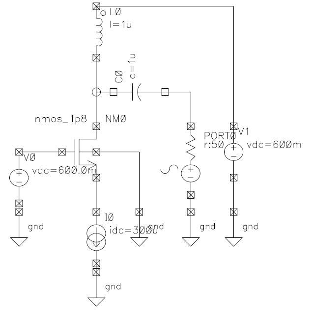
As you can see, the current is fixed by the ideal current source at the source of the transistor. I used S-Parameter analysis and plotted Z11 in magnitude. Thus is contains both the real and imaginary component. I am using the 0.18 um process and the PDK i'm using has so far proven to be reliable enough.

Sweep           Dependence
-------            --------------
VGS              weak
IDC               weak
VDD              weak
L                   quite weak
Fingers          weak*
W                  Strong

So from the data i found that by far the biggest factor in determining the output impedance was the transistor width. Is this a well known phenomenon? I thought that at 2.45 GHz the transistor would still roughly follow the DC solution.

The strange thing is that when i ran a simulation of output impedance versus IDC for a full LNA, I found it to roughly follow the 1/IDC curve. So anybody know what i've been doing wrong or what's going on?

thanks,
Aaron

Back to top


there is no energy in matter other than that received from the environment - Nikola Tesla
View Profile   IP Logged
aaron_do
Senior Fellow
******
Offline


Posts: 1398

Re: RF NMOS output impedance
Reply #1 - Nov 9th, 2006, 12:02am
 
haha...oops. I figured it out...never mind

Aaron
Back to top


there is no energy in matter other than that received from the environment - Nikola Tesla
View Profile   IP Logged
eng
Community Member
***
Offline


Posts: 49
USA
Re: RF NMOS output impedance
Reply #2 - Nov 27th, 2006, 10:04am
 
Hi Aaron,
Could you please share the answer as well?

thnx
eng
Back to top
 
 
View Profile   IP Logged
aaron_do
Senior Fellow
******
Offline


Posts: 1398

Re: RF NMOS output impedance
Reply #3 - Nov 27th, 2006, 4:21pm
 
Hi Eng,

my simulation setup is wrong. The real part of the output impedance is infinite since the ideal current source adds infinite real resistance. Therefore the magnitude of the output impedance only depends on the imaginary part which is Cgd (proportional to the width).

Back to top


there is no energy in matter other than that received from the environment - Nikola Tesla
View Profile   IP Logged
ACWWong
Community Fellow
*****
Offline


Posts: 539
Oxford, UK
Re: RF NMOS output impedance
Reply #4 - Nov 28th, 2006, 3:56am
 
So do you short out I0 with a shunt ideal cap?  if so do you balance the vds/idc to ensure the source is at ground in a DC simulation to give you 600mV vds ?
I usually bias NM0 off a mirror to set the current, this way you know NM0 source is at ground always and zero degeneration or vbs exists, and you get the vds you put in V1 without having to juggle vgs as well.
Back to top
 
 
View Profile   IP Logged
aaron_do
Senior Fellow
******
Offline


Posts: 1398

Re: RF NMOS output impedance
Reply #5 - Nov 28th, 2006, 4:54am
 
Hi aw,

yeah thanks...after I realised my mistake I removed the ideal current source. Then I just swept the gate bias voltage and used excel to plot Rout versus Ids. The current mirror method you mentioned also sounds like a good idea...don't need to use excel. I guess you need to add another ideal cap to AC ground the gate...

Actually I think I tried the current mirror method too, but the mirror doesn't seem give a perfect 1 to 1 relationship between the currents. More accurate to use the excel method...

Aaron
Back to top


there is no energy in matter other than that received from the environment - Nikola Tesla
View Profile   IP Logged
ACWWong
Community Fellow
*****
Offline


Posts: 539
Oxford, UK
Re: RF NMOS output impedance
Reply #6 - Nov 28th, 2006, 6:41am
 
yes you don't get 1:1 so i usually just sweep Ibias to the mirror to find the value i want in NM0...
also yes you can add a cap to the gate if you want a low impedance on the gate.... to match your vdc vgs drive you'll probably need it to match the results closely.

Back to top
 
 
View Profile   IP Logged
Pages: 1
Send Topic Print
Copyright 2002-2024 Designer’s Guide Consulting, Inc. Designer’s Guide® is a registered trademark of Designer’s Guide Consulting, Inc. All rights reserved. Send comments or questions to editor@designers-guide.org. Consider submitting a paper or model.